The rise of data-centric computing, increasingly large data sets, and the convergence of traditional high-performance computing with big data and real-time data analytics, is driving significant development in memory technology. This has led to several technologies that are changing the long-established architectures of HPC, from the introduction of 3D memory to some unconventional technologies which are blurring the lines between compute, memory and storage.
One of the biggest challenges to a sustained increase in application performance is the ability to move data either from memory or storage into the computational elements of a cluster.
Each jump – from computation to memory and then from memory to storage – has an associated latency, as David Power, head of HPC at Boston explains. ‘If you look at the hierarchy of I/O you have the small caches [of memory] on the CPU. You then have a latency penalty going to main memory but as you go to the next level of I/O, which would be your disk layer, suddenly the latency and your performance are orders of magnitude slower than you would get from memory or cache.’
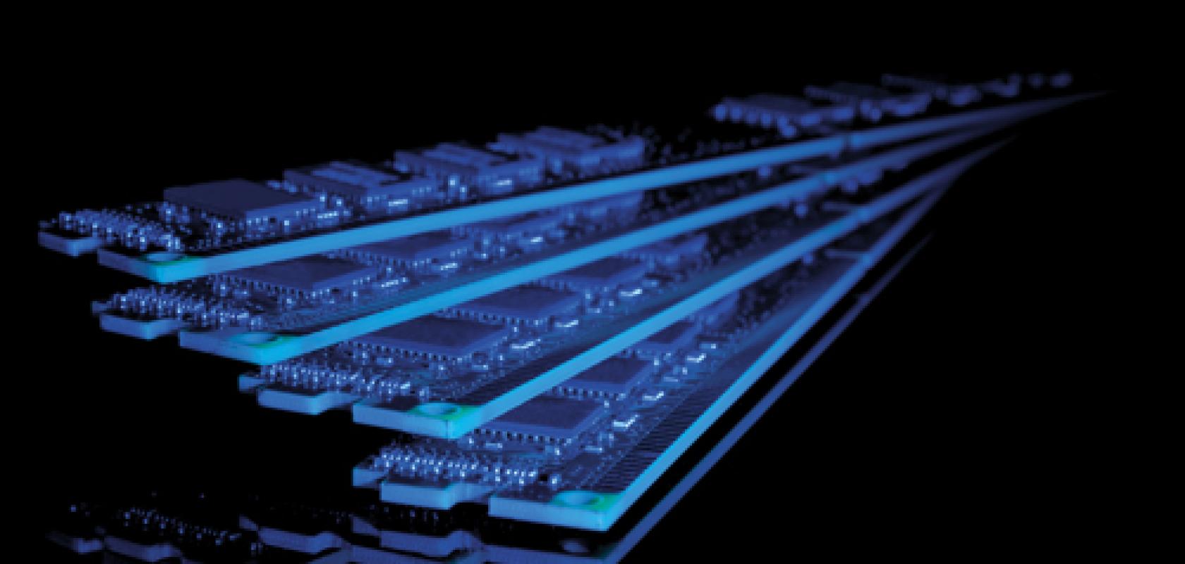
This I/O latency, combined with the huge increases in processing power, means that many HPC users now find themselves in a situation where application performance is bound to memory bandwidth – the rate at which data can be read from or stored into a semiconductor memory by a processor).
Balancing the HPC ecosystem
To keep pace with developments in processor technology, memory companies are exploring changes to current HPC architectures. One idea is to bring data closer to computation; an example of this is Diablo Technologies, a memory specialist and partner of Boston.
Diablo has created a storage medium that connects through the DIMM sockets used for system memory. This considerably reduces the latency penalty when compared to traditional storage mediums, as the storage is running through the same network interface as memory so it has the same associated latency.
‘We have been engaged with Diablo for a number of years, we have had their products in the lab and have been engineering solutions with them’ said Power. ‘What Diablo is doing is integrating storage onto a memory form factor. We can, in effect, put a storage system into our memory DIMMs and provide that at the same sort of performance of latency to the overall architecture, as opposed to going through SATA controllers and onto rotational disk.’
‘It’s kind of like SSDs on steroids for making sure that you have a well-balanced architecture’ concluded Power.
Another company that is trying to make significant changes to memory technology is the memory manufacturer Tezzaron. Tezzaron specialises in designing and manufacturing memory using transistor-level 3D technology. This strategy focuses on stacking transistors instead of just making them smaller. These stacked circuits are called ‘3D-ICs’.
David Chapman, VP of marketing for Tezzaron, said: ‘The Tezzaron method requires changes on several different fronts simultaneously; basic chip architecture, circuit design, debug, test and packaging. Naturally, that includes new silicon processing techniques as well.’
Tezzaron stacks complete wafers before they are cut into individual dies, hence the term – wafer level stacking. These wafers are then thinned by grinding down the unnecessary material; the circuits are on the face of the wafer, so the wafer is put on the turntable face-down, and the blank backside is ground away.
This process must be handled carefully because if a wafer gets too thin, it becomes weakened. To overcome this, Tezzaron bonds two wafers together, face-to-face. This enables the company to produce stacks of wafers much thinner than is normally possible. Tezzaron claims that they can create memory wafers that are approximately 1/10 the thickness of wafers produced by their competitors.
Another technique that Tezzaron employs during the manufacture of its memory is the use of extremely small tungsten contacts connecting these wafers. The small wafers enable the use of smaller contacts, and this allows up to 100 times as many vertical wires throughout the memory stack.
Although this manufacture method is slightly more expensive, Chapman believes this will be minimised at sufficient scale. ‘We believe that, once in volume, it will be significantly cheaper. The technology will become relatively less and less expensive over time, as other approaches to increasing transistor density per unit area of silicon continue to rise in cost at an exponential rate.’
Because Tezzaron has so many vertical wires in the chip, there are more connections available for fine-grained repair. That means that more defects can be repaired in each chip. These intricacies enable the company to design built-in self-test and repair technology BiSTAR.
While increasing memory bandwidth is the most obvious option to increasing application performance. Micron, a provider of memory and storage products, has been working on a new emerging technology called Automata Processing. This project focuses on reducing the amount of data that needs to be moved across the network into the CPU, rather than increasing memory bandwidth.
‘You can think of this as being a massive regular expression pattern matching engine. Before you need to move the data onto the CPU to do the computation or check against it you can cleanse a massive amount of information in regular expressions before it even gets to the CPU’ said Power.
Power explained that Boston has been working with some early prototypes of this technology: ‘This is another product that we have in the lab that could potentially revolutionise the way that memory is used.’
He explained that, in its first incarnation, this technology would be a PCI add-on, but future generations would likely be based on a memory DIMM form factor.
‘This is a hugely exciting area of research that we are engaged in with Micron. It could have major implications for any application that is big data or analytically orientated’ said Power.
Micron’s Automata Processor (AP) is a programmable silicon device, capable of performing high-speed, comprehensive search and analysis of complex, unstructured data streams. Unlike a conventional CPU, the AP is a scalable, two-dimensional fabric comprised of thousands of interconnected processing elements, each programmed to perform a targeted task or operation.
The Automata Processor PCIe board is the first platform to host Micron’s Automata Processor technology. The design uses an Altera FPGA to bridge a communication interface between a host server and several ranks of Automata Processors on two different channels.
Although the technology is still in development, Micron released an SDK earlier this year. The SDK includes a visual development environment, compiler, design rules checker, and simulation tools, to enable developers to build, compile, simulate, and debug their designs.
Another project set to make a large impact on the HPC industry is based on collaboration between Intel and Micron. The technology, known as 3D XPoint, is a new class of non-volatile memory. Intel has claimed that throughput could be up to 1,000 times higher than flash memory.
This technology, similar in concept to Diablo’s memory storage technology, will enable high-speed, high-capacity data storage close to the processor, significantly decreasing latency compared to today’s technology.
‘This could potentially eradicate the need for a storage back-end. There is a scenario where you would see a hybrid back-end comprised of memory and storage that will use memory as your main storage rather than having a third tier of disk’ explained Power.
Shifting paradigms of HPC
The memory subsystem is the fastest component of an HPC cluster outside of the processing elements. But, as Power explains: ‘When you are looking at very large distributed workloads, the vast majority of your time can be spent just moving bits around, moving data around the place.’
Data sets are growing at an unprecedented rate and the while CPUs, and other processing elements are doubling in speed in accordance with Moore’s law, the demand for data is outstripping our ability to feed the CPU. This demand necessitates that memory company’s look beyond iterative development to more disruptive technologies.
Automata Processing ‘is a great technology; it can site even quite large databases and accelerate applications by an order of magnitude just due to the increased throughput and IOPS capabilities. Optimising that part of the workflow in your application can have significant gains when you are starting to look at large-scale computing’ said Power.
A move away from commodity hardware
The importance of memory to the next-generation HPC application is clear as David Chapman, VP of marketing at Tezzaron explains: ‘How important are brakes to winning an F1 race? They may not do much to increase your speed on the straights, but surviving the corners is fairly critical to winning. My point is that the whole system has got to work well.’ While the CPU and accelerators maybe be doing the computation without a balanced system to support this computation, application performance will suffer.
‘Having said that, it seems clear (to me at least) that the memory industry has been on an Intel/PC-centric path for so long that all other application environments have found themselves with a very narrow and largely unsuitable selection of memory devices.’ Chapman went on to explain that they are unsuitable because ‘RAM performance characteristics demanded by PC applications are not optimum for other applications.’
As we have seen from the emerging memory technologies, the answer to HPC’s memory problems may lie in the development of bespoke technologies designed specifically for big data or large-scale HPC. ‘HPC really means “workloads that PCs don’t do very well.” From that point of view it is unsurprising that HPC needs different memory from commodity memory for PCs’, said Chapman.
The likely path for memory technology over the next five to 10 years will be technology designed specifically to address the convergence of HPC and big data. Exotic technologies that disrupt the current design of HPC systems are already being readied to support the next generation of HPC systems.
‘The prominent trend for memory over the next 20 years is going to be fragmentation’ said Chapman. ‘Although memory standards may not go away, they will be confined to the very slow end of the market, which always includes the consumer market, where price always carries the day.’
‘The parts of the market where system vendors thrive on performance differentiation first and price differentiation second will more and more readily embrace differentiated memory as a key tool for keeping their competitive edge sharp. In short, non-commodity memory fabricated with transistor-level 3D techniques will be one of the most visible trends in HPC going forward’, concluded Chapman.
Another trend is that of fragmenting the established subsystems of a cluster. Power explained that there are two main directions in which he sees memory technology evolving. The first, 3D Cross Point ‘leverages advances in science and component physics to make memory faster and larger. But, what Micron is doing is almost the reverse. Rather than bringing everything closer to the CPU and making it faster, they are taking computational capabilities out of the CPU so you have another computational tier within your overall architecture.’
‘You can see how the traditional structure of a cluster is being turned on its head, and you will now see computational elements throughout the architecture. It is going to be fun to try and programme for all of that’, concluded Power.
