A team of researchers at Lawrence Berkeley National Laboratory (Berkeley Lab) and UC Berkeley have identified one energy-efficient route to developing ultrathin transistors – by synthesising a thin-layer version of a well-known material whose properties are exactly what’s needed for next-generation devices. The findings were published in the journal Nature Materials.
First discovered more than 80 years ago, barium titanate (BaTiO3) found use in various capacitors for electronic circuits, ultrasonic generators, transducers, and even sonar.
Lane Martin, a faculty scientist in the Materials Sciences Division (MSD) at Berkeley Lab and professor of materials science and engineering at UC Berkeley who led the work comments: ‘We’ve known about BaTiO3 for the better part of a century and we’ve known how to make thin films of this material for over 40 years. But until now, nobody could make a film that could get close to the structure or performance that could be achieved in bulk.’
BaTiO3 Crystals respond quickly to a small electric field, flip-flopping the orientation of the charged atoms that make up the material in a reversible but permanent manner even if the applied field is removed. This provides a way to switch between the proverbial '0' and '1' states in logic and memory storage devices – but still requires voltages larger than 1,000 millivolts (mV) for doing so.
Seeking to harness these properties for use in microchips, the Berkeley Lab-led team developed a pathway for creating films of BaTiO3 just 25 nanometers thin – less than a thousandth of a human hair’s width – whose orientation of charged atoms, or polarization, switches as quickly and efficiently as in the bulk version.
Historically, synthesis attempts have resulted in films that contain higher concentrations of ‘defects’ – points where the structure differs from an idealised version of the material – as compared to bulk versions. Such a high concentration of defects negatively impacts the performance of thin films. Martin and colleagues developed an approach to growing the films that limits those defects.
To understand what it takes to produce the best, low-defect BaTiO3 thin films, the researchers turned to a process called pulsed-laser deposition. Firing a powerful beam of ultraviolet laser light onto a ceramic target of BaTiO3 causes the material to transform into a plasma, which then transmits atoms from the target onto a surface to grow the film. “It’s a versatile tool where we can tweak a lot of knobs in the film’s growth and see which are most important for controlling the properties,” said Martin.
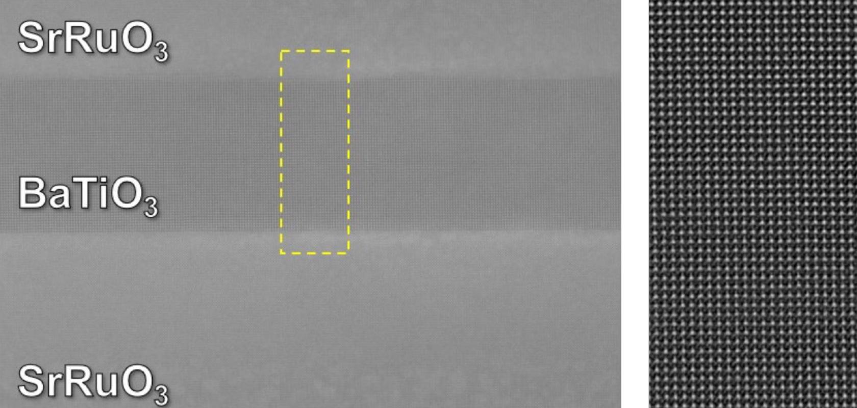
Martin and his colleagues showed that their method could achieve precise control over the deposited film’s structure, chemistry, thickness, and interfaces with metal electrodes. By chopping each deposited sample in half and looking at its structure atom by atom using tools at the National Center for Electron Microscopy at Berkeley Lab’s Molecular Foundry, the researchers revealed a version that precisely mimicked an extremely thin slice of the bulk.
‘It’s fun to think that we can take these classic materials that we thought we knew everything about, and flip them on their head with new approaches to making and characterising them,’ said Martin.
Finally, by placing a film of BaTiO3 in between two metal layers, Martin and his team created tiny capacitors – the electronic components that rapidly store and release energy in a circuit. Applying voltages of 100 mV or less and measuring the current that emerges showed that the film’s polarisation switched within two billionths of a second and could potentially be faster – competitive with what it takes for today’s computers to access memory or perform calculations.
The work follows the bigger goal of creating materials with small switching voltages, and examining how interfaces with the metal components necessary for devices impact such materials. 'This is a good early victory in our pursuit of low-power electronics that go beyond what is possible with silicon-based electronics today,' said Martin.
‘Unlike our new devices, the capacitors used in chips today don’t hold their data unless you keep applying a voltage,’ said Martin. And current technologies generally work at 500 to 600 mV, while a thin film version could work at 50 to 100 mV or less. Together, these measurements demonstrate a successful optimisation of voltage and polarisation robustness – which tend to be a trade-off, especially in thin materials.
Next, the team plans to shrink the material down even thinner to make it compatible with real devices in computers and study how it behaves at those tiny dimensions. At the same time, they will work with collaborators at companies such as Intel to test the feasibility in first-generation electronic devices. ‘If you could make each logic operation in a computer a million times more efficient, think how much energy you save. That’s why we’re doing this,’ said Martin.
This research was supported by the US Department of Energy (DOE) Office of Science. The Molecular Foundry is a DOE Office of Science user facility at Berkeley Lab.
