First- and second-generation GPGPUs for HPC applications have been based to a large extent on the architecture from which the chips get their name: graphics. While current GPGPUs boost some HPC applications tremendously (see references), they haven’t been optimised for the data-crunching involved in scientific processing and have displayed a few weak points. These weak points are now being eliminated.
The key driver behind this upcoming major jump in performance is Nvidia – for two reasons. This company, which presently dominates the GPGPU market, has announced its new Fermi architecture, scheduled for shipment in Q2 2010. Second is Intel’s recent announcement that development of its Larrabee (a hybrid between a multi-core CPU and a GPU) is behind schedule; as a result, the first Larrabee product will not be launched as a stand-alone discrete product as originally intended, but rather in the form of a software-development platform for internal and external use.
Remove the weak points
Fermi is a totally recast architecture, representing what the developer terms ‘the world’s first computational GPU’. It removes all the major HPC-related weaknesses of the current generation. Fig. 1 summarises the differences between the G80 (the original GPGPU from 2006), the GT200 architecture that is the basis for the current Series 10 products, and the upcoming Fermi architecture, which will be featured in Series 20 products. Some are ‘behind-the-scenes’ improvements that, while important, are largely transparent to users. A few, however, will be of great interest to HPC users, and they include accelerated double-precision performance, a new memory architecture including shared memory, support for ECC (error-correcting code) and enhanced programming tools.
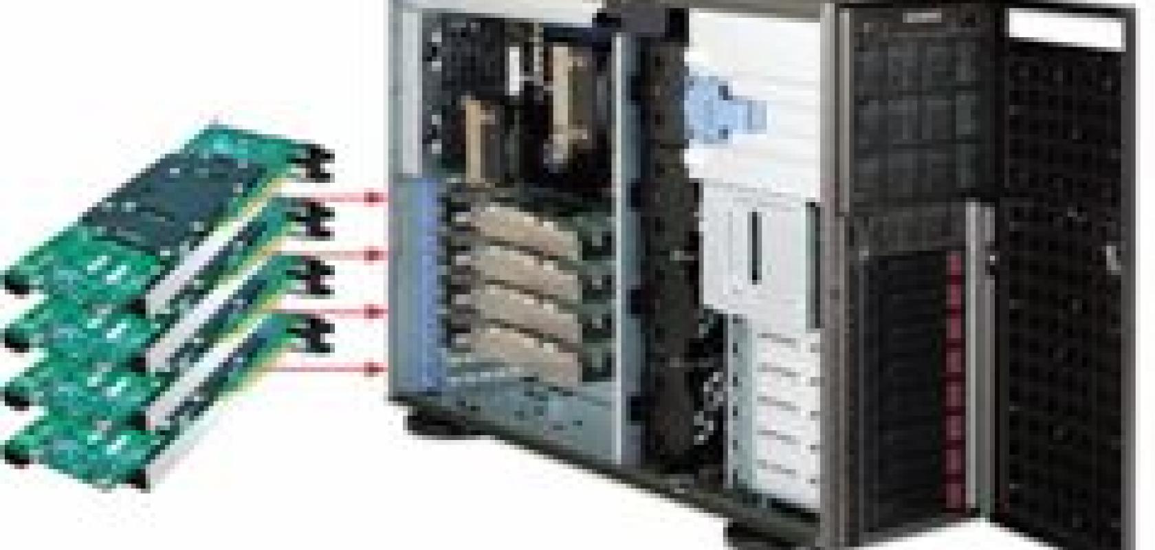
Even better, there are few downsides to these improvements. For instance, although current GPU plug-in cards are known for the relatively large amounts of power they draw (typically 165W), the increase for cards based on the new architecture at roughly 190W is modest, and most Cuda applications, states Sumit Gupta, senior product manager at Nvidia, will fall below that level. Most system integrators share the opinion of the company Boston, which reports that no changes will be necessary in its existing platforms in terms of cooling, power supplies or expansion slots, thus allowing customers to take advantage of this new technology at the earliest opportunity. For its range of platforms, the new Tesla 20 Series cards based on Fermi will essentially be drop-in replacements.
Larger chip; larger memory
Returning to the table, examine some of the basic architectural improvements. Start with the fact that the number of transistors has more than doubled, and the chip now features as many as 512 Cuda cores (each of which executes an integer or floating-point instruction per clock for a particular thread). These cores are organised in 16 streaming multiprocessors (SMs) each with 32 cores. The GPU has six 64-bit memory partitions for a 384-bit memory interface and supports up to 6GB of GDDR5 DRAM. A host interface connects the GPU to the CPU over a PCI-Express link. Finally, the GigaThread global scheduler distributes thread blocks to the SM thread schedulers.

Summary of the G80 architecture (from 2006), the GT200 architecture (now being used) and the upcoming Fermi architecture.
Shared memory has been a big request from HPC users according to Nvidia’s Gupta. The Fermi architecture implements a single unified memory request path for loads and stores, and it provides an L1 cache per SM and a unified L2 cache that services all operations (load, store and texture). Algorithms for which data addresses are not known beforehand, and which have irregular accesses to the same data, especially benefit from this new cache hierarchy. Such algorithms include ray tracing, sparse-matrix multiplication, finite-element analysis as well as computational fluid dynamics and similar physics solvers.
Leading to improved performance
Another aspect of improved performance and accuracy are the streaming multiprocessors (SMs), which have four times as many Cuda cores as the predecessor. Each Cuda processor has a fully pipelined arithmetic logic unit (ALU) and floating-point unit (FPU). Prior GPUs used IEEE 754-1985 floating-point math, but Fermi implements the IEEE 754-2008 standard. Thus it provides the fused multiply-add (FMA) instruction for both single- and double-precision maths. FMA improves over a multiply-add (MAD) instruction by doing the multiplication and addition with a single final rounding step with no loss of precision in the addition.
In the current GT200 architecture, the integer ALU is limited to 24-bit precision for multiply operations; as a result, multi-instruction emulation sequences were required for integer arithmetic. In Fermi, the new ALU supports full 32-bit precision for all instructions, and it is also optimised to support 64-bit and extended-precision operations efficiently.
Note, also, that the Fermi doubles the number of special function units (SFUs), which execute transcendental instructions such as sine, cosine, reciprocal and square roots. Each SFU executes one instruction per thread, per clock.
The addition of bit error correction
A significant addition to the Fermi architecture is ECC; register files, shared memories, L1/L2 caches and DRAM are ECC protected. According to Nvidia, it’s the first GPU to support ECC-based protection of data in memory. ECC takes up five to 10 per cent of the chip die, which for a processor represents a huge investment – but it shows that Fermi has HPC applications in mind.
Why is ECC so important? Naturally-occurring radiation reaching the earth’s surface and travelling through buildings and computer chassis can cause a bit stored in RAM to be altered, resulting in a soft error. Fermi supports SECDED (single-error correct double-error detect) codes that correct any single-bit error in hardware as the data is accessed. SECDED also ensures that all double-bit errors and many multi-bit errors are also detected and reported so that the program can be re-run rather than being allowed to continue executing with bad data.
Graphics applications, where GPUs have their roots, are forgiving in this regard, because users don’t notice a bit error. But in data computation, a lost bit can be a very big issue. ECC is a necessary ingredient in scientific computing, says Oliver Tennert of system integrator Transtec. In applications such as the simulation of nuclear detonations, for instance, bit error propagation can have a very large impact.
Many customers, especially those just getting into GPUs, haven’t realised until now that existing Nvidia GPUs have no ECC, although long-time users did know about that omission, relates David Yip, new technology business development manager at system integrator OCF. He adds that certain branches, such as metrological offices, haven’t considered even touching GPUs until now due to possible cascading errors, but that will now change.
Some customers, adds Transtec’s Tennert, have known that there was no ECC, but have taken it into account. For the right problems, the performance boost is great and the demand for Tesla products has been growing; he relates that until now the better part of Transtec’s customers have purchased only from one to four GPUs where the chance of a bit error is quite small. However, when a process involves many GPUs, the probability of a bit flip goes up linearly – so, for large installations, ECC becomes very important. Because the probability of soft errors increases with the number of installed systems, ECC is essential in large clusters.
Faster double-precision
While double-precision (DP) maths isn’t new to GPUs, with Fermi it reaches levels that make it much more useful. DP maths is at the heart of HPC applications, such as linear algebra, numerical simulations and quantum chemistry. In the Fermi architecture, as many as 16 double-precision FMA operations can be performed per SM per clock. In practical terms, this means that a typical double-precision matrix runs approximately four times faster than in the GT200 implementation. Put another way, double-precision previously took eight times as long as single-precision calculations, but now it’s just half of the time. Due to this speed-up, highly double-precision bound applications will enjoy a huge benefit, up to eight times the performance. In the last few years, many applications have used single-point precision and switched over to double-precision only when really needed for convergence, but now they can run DP maths all the time.
New software-development options
Writing code for GPUs hasn’t been trivial, and development tools are critical, because so many GPU users are developing custom programs. Transtec’s Tennert reports that some 95 per cent of his Tesla customers are in an academic environment and write their code. He believes that the first adopters writing code are always in the academic world, where much GPU activity is taking place, and that the technology then trickles down to widespread usage.

Improved double-precision maths is helping maintain the sharp rise in the GPU performance curve.
Users writing programs should be pleased to learn that the launch of Fermi coincides with a new integrated development environment for Microsoft’s Visual Studio, code named Nexus. It is claimed to bridge the productivity gap between CPU and GPU code by bringing parallel-aware hardware source code debugging and performance analysis directly into Visual Studio. With that environment, developers can now write and debug GPU source code, including source and data breakpoints, and inspect memory contents.
Further, Nexus extends Visual Studio functionality by offering tools to manage massive parallelism such as the ability to focus and debug on a single thread out of the thousands of threads running in parallel, and the ability to visualise the results computed by all parallel threads. Nexus captures performance events and information across both a CPU and GPU, and it presents the information to the developer on a single correlated timeline. Developers can see how an application behaves on the entire system rather than through a narrow view focused on a particular subsystem or processor.
There has been some confusion concerning these two primary ways to program GPUs: with Cuda or OpenCL. ‘When we started the GPU revolution,’ says Gupta, ‘there was no way to program a massively parallel device such as ours, so we had to come up with a programming tool.’ The result was Cuda, which is a C compiler with keyword extensions. Since then, Apple has proposed OpenCL as a general API for the same purpose.
Nexus doesn’t support OpenCL at this time because, according to Gupta, Cuda development started prior to OpenCL, but this functionality is a ‘roadmap item’. In addition, Cuda has a large developer base, which Nvidia is watching closely. The company emphasises its heavy involvement with OpenCL, saying they have taken a front seat in enabling developers to use that as well as its own tools. For instance, Nvidia chairs the working group, indicates it was the first to pass OpenCL driver conformance and the first to get drivers into developers’ hands. The firm also states that it is still the only vendor supporting OpenCL features beyond the minimum conformance level such as double precision and OpenGL interoperability.
People who write applications for visualisation do so with OpenGL, and OpenCL uses the same programming style so there is less of a transition. In addition, that API gives you more control over the hardware, because you in essence write code at a lower level. In the scientific world, though, people prefer higher level programming such as Matlab over C++. These people are thus attracted to Cuda C, Cuda Fortran and now Cuda C++.
It’s also important to note that existing Cuda binaries will run on Fermi, because at runtime the new driver recompiles the Cuda assembly code and will even take advantage of the new features. There’s no need to recompile applications unless programmers want to move more tasks to the GPU.
Ready for takeoff
With the major obstacles to technical computing removed from GPUs, suppliers are getting very excited. David Yip of OCF expects his company to sell much more GPU-based hardware this year. In the past, users have sourced one or two units, but with Fermi, GPU computing is definitely moving into mainstream and cluster systems. Last year he saw two or three clusters with GPUs attached, but he expects this year to be different. He looks back upon 2009 as the year in which GPUs made their entry into supercomputing, but with Fermi, GPUs will take a far bigger step. Scientific computing users will take a serious look at it, and it will also attract the interest of more ISVs.
The increase in computational power provided by the new GPU architecture is indeed significant, concurs Neil Kalsi, sales manager at Boston. He notes that their Venom T4000 GPU PSC compute platform will support as many as 2,048 GPU compute cores within one workstation/4U enclosure.
A computational inflection point
With Fermi, Nvidia’s Gupta believes that we’ve reached an inflection point in the use of GPU technology. He makes a comparison to the Model T, where everyone could suddenly have an automobile; with the smart phones, there was suddenly a PC in everyone’s hand. He sees the same thing happening in computing: the Fermi puts a device with the power of a supercomputer in every engineer’s hands.
Schreier, P., “A supercomputer chip for every man”, Scientific Computing World, Feb/Mar 2009, pgs 30-32.
