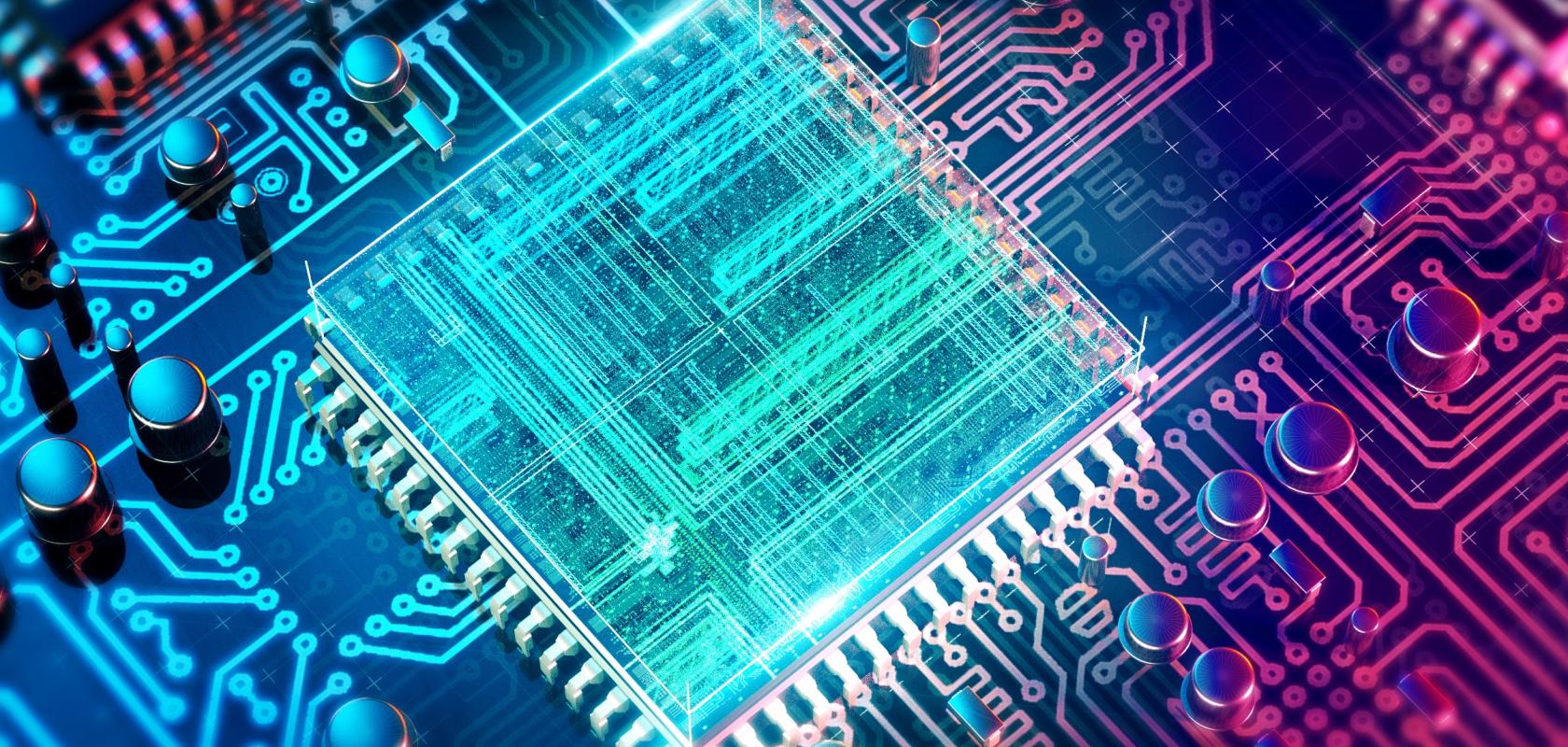
Photonic computing technologies are seeing rapid growth in research output and technology development, and products are now entering the market. How will this new computing revolution impact scientists and engineers' research capabilities?
Photonic technology offers enormous potential advantages to data processing speeds for large-scale computing infrastructure while also promising to reduce networking and communications energy consumption. This technology has huge ramifications for advanced computing infrastructure such as supercomputers (HPC and AI), cloud computing, data centre networking and even quantum computing.
Performance bottlenecks and energy efficiency are a growing concern for scientists and researchers using HPC and AI systems as they can potentially limit application performance or make large scale computing unsustainable.
More efficient AI
In March 2023, Oxford University spinout Lumai was awarded £1.1m Innovate UK Smart Grant to power to commercialise its work in all-optical network training and deep optics for faster, more efficient computing.
Spinning out of The University of Oxford in January 2022, Lumai is developing all-optical neural networks for next-generation AI. With £1.1m in Smart funding, the company is creating advanced optical computing processors where the information flow and calculations are not dependent on electronic processing. The Grant was awarded in conjunction with The University of Oxford and follows its previous funding from IP Group and Runa Capital.
Existing transistor-based digital electronics are struggling to support the potential offered by AI, especially with the explosive increase of computation demand to support breakthrough AI models such as ChatGPT. To combat this, Lumai’s computing platform is capable of energy-efficient and ultra-fast parallel processing. Lumai’s optical neural networks can be 1000x faster – and much more sustainable – than existing transistor-based digital electronics.
The funding will support Lumai in building and launching optical neural networks for high-performance computing and machine vision, while simultaneously leading developments in advanced optical technologies.
Accelerating HPC and GPU computing
The continued scaling of HPC and AI systems relies on significant energy efficiency increases. Today’s largest supercomputers can consume as much as 20 megawatts and with the continued demand for AI, energy demand may rise.
Reducing energy efficiency is not a new concept for HPC system providers or those that manage or provision HPC clusters. For many years a 20 MW power envelope has been discussed for exascale computing. Frontier may have missed the 20-megawatt target by a small margin, but the system demonstrates how far the HPC industry has come in developing efficient HPC systems. For example, The Sunway TaihuLight supercomputer was the world's most powerful system when it launched in 2016. In the November 2022 edition of the Top500, this system is now in #7 spot delivering a peak performance of 93 PFlop/s (petaflops per second) with a power consumption of 15,371 kW (15.3 MW). By comparison, the LUMI system, launched in 2022, delivers almost three times the performance of Sunway TaihuLight at 309 PFlop/s but consumes just a fraction of the power at 6,016 kW (6.0 MW).
However, as HPC cloud and AI computing continue to grow, more scientists and researchers are getting access to advanced computing infrastructure. There is still significant growth in the cloud and AI markets. As the demand for AI supercomputers grows, steps must be taken to make the technology more sustainable.
Several key market verticals in life sciences, such as biotechnology and pharmaceuticals, are shifting towards the use of AI for image classification of medical images and to aid in the search for new drugs and treatments. In engineering, there has been a shift from traditional testing and validation to complex digital twins and with comprehensive digital verification and testing in simulation. The Automotive market is also seeing demand for training large scale models for autonomous driving and the use of AI in other applications such as topology optimisation. Compounding this effect in science and engineering is the growth of data intensive workloads.
Integrating photonic technologies into classical commuting could help to significantly reduce the power budgets of moving data across systems. While this may seem insignificant training of AI models requires large amounts of data
Photonic computing promises to open up new possibilities for data transfer and communications between computing elements which could significantly increase HPC performance. Several early players have merged in this market with technologies that could find their way into future supercomputers.
Lightelligence is an MIT spinout using photonics to reinvent computing for artificial intelligence. The company launched its first fully integrated optical computing platform PACE (Photonic Arithmetic Computing Engine) in 2021. PACE leverages the inherent properties of light to generate optimal solutions to the Ising, Max-Cut, and Min-Cut problems over 800 times faster than current high-end GPUs while maintaining high throughput, low latency, and energy efficiency.
In a 2021 interview with MIT News, LightIntelligence CEO Dr Yichen Shen commented: “We’re changing the fundamental way computing is done, and I think we’re doing it at the right time in history. We believe optics will be the next computing platform, at least for linear operations like AI.”
The PACE platform also has the potential for use in autonomous driving systems and has shown to be more powerful than high-end GPUs in some applications. “Our chip completes these decision-making tasks at a fraction of the time of regular chips, which would enable the AI system within the car to make much quicker decisions and more precise decisions, enabling safer driving,” says Shen.
The core technology that underpins PACE is a 64x64 optical matrix multiplier in an integrated silicon photonic chip and a CMOS microelectronic chip, flipchip packaged together. In addition to its advanced 3D packaging, PACE's photonic chip contains over 12,000 discrete photonic devices and has a system clock of 1GHz.
Overcoming the memory bottleneck
In 2022, Hewlett Packard Enterprise and Photonic computing startup Ayar Labs recently signed a multi-year strategic collaboration to accelerate the networking performance of computing systems and data centres by developing silicon photonics solutions based on optical I/O technology. This was soon followed by news that Ayar Labs had secured $130m in additional funding from Boardman Bay Capital Management, Hewlett Packard Enterprise (HPE) and Nvidia, as well as multiple new and existing financial investors, which include GlobalFoundries and Intel Capital.
Silicon photonics will enhance networking capabilities and support future requirements for high performance computing (HPC), artificial intelligence (AI), and cloud computing architectures. The technology also has the potential to reduce the amount of energy used in data centres and large computing systems.
Hugo Saleh, Ayar Labs' senior vice president of commercial operations, stated: “Whether you’re talking about HPC, or disaggregated computing, there is a real limiter on I/O.’ said Saleh. “In HPC, it’s usually referred to as a memory bottleneck. It’s not a memory capacity issue. It’s the ability to move the data from memory DIMMs into the CPU and back. The other bottleneck that’s been seen and talked about quite a bit is the bottleneck on the GPU. Between the CPU and GPU transferring the data and then again, between the GPU itself and the memory.”
“What we do at Ayar Labs is an attempt to change the physical domain that data is transmitted,’ noted Saleh. ‘Going from electricity, voltages and currents, to photons. And we do that coming straight out of the socket. So it’s not a transceiver at the back of the server, it’s not a mid-board optics. We design chiplets that sit inside the package, nearly abutted to the CPU, memory, GPU or accelerator. We’re agnostic to the host ASIC. Then we transmit photons and light outside of the package for your high speed, low power I/O.”
Ayar Labs first demonstrated this technology at Supercomputing 2019, the US conference and exhibition held annually in the US. “We have a full test rig. We first demonstrated our technology to the HPC community at Supercomputing 2019 in Denver. Since then we’ve made two public announcements about the projects we’re doing with Intel. So Intel has themselves demonstrated an FPGA with our photonics inside of it, transmitting massive amounts of data at much lower power,” stated Saleh.
This technology could massively increase the memory bandwidth for future HPC and AI systems. Each chiplet delivers the equivalent of 64 PCIe Gen 5 lanes, which provides up to two terabits per second of I/O performance. The system uses standard silicon fabrication techniques and disaggregated multi-wavelength lasers to achieve high-speed, high-density chip-to-chip communication with power consumption at a picojoule range. Ayar Labs developed its technology alongside GlobalFoundries as part of its monolithic silicon photonics platform.
“We worked with the GlobalFoundries on developing a monolithic process, one that lets you put electronics and optics on the same chip,’ Saleh said. ‘A lot of traditional optics are separate; we have it all combined into one, and that simplifies our customer’s life when they’re packaging all these components – it reduces power, costs, and latency.”
GF Fotonix is Global Foundries’ next-generation, monolithic platform, which is the first in the industry to combine its 300mm photonics features and 300GHz-class RF-CMOS on a silicon wafer. The process has been designed to deliver performance at scale and will be used to develop photonic compute and sensing applications. Ayar Labs also helped GF develop an advanced electro-optic PDK that will be released in Q2 2022 and will be integrated into electronic design automation (EDA) vendor design tools.
Dell backs photonic quantum computing startup
In April, an Israeli photonic quantum computing startup announced it has extended its seed funding round to $27 million - thanks to an injection of cash from Dell Technologies Capital (DTC). Quantum Source, which aims to develop commercially viable photonic quantum computers, will use the $12 million top-up to expand its research and development team as it scales to reach significant technical and performance milestones.
In this context photonic quantum computing uses photons as a representation of qubits. Quantum Source uses a unique approach to generate photons and quantum gates up to five orders of magnitude more efficiently than state-of-the-art implementation.
Oded Melamed, co-founder and CEO of Quantum Source, comments: “We founded Quantum Source with the belief that photonic quantum technologies are the best route to achieve large-scale, fault-tolerant quantum computers. Our unique approach will dramatically improve the scalability of those machines and will be the key to commercial success of quantum computers. Having investors such as Dell Technologies Capital believe in us will allow us to accelerate our work and by extension, entire industries.”
Founded in 2021 by a team of semiconductor industry veterans and accomplished physicists, Quantum Source is developing technology to efficiently implement large scale, fault-tolerant, photonic quantum computers. To date, companies have built small quantum computers with just tens or hundreds of qubits. While these rudimentary quantum computers are truly groundbreaking technology, the systems are not yet commercially viable.
Omri Green, partner at Dell Technologies Capital, comments: “DTC invests in technologies that can move industries forward. We believe quantum computing has this potential and, as our first investment in this area, Quantum Source can be the team to get us there. Oded and this exceptional team of scientists and proven entrepreneurs are addressing crucial hurdles in photonic quantum – scalability and fault tolerance. Once those challenges are solved, the innovation upside will be boundless.”
UK-based ORCA Computing, which develops photonic quantum systems for machine learning. ORCA raised $15 million last year and is leading a research project to develop a “quantum data centre”. Other firms working on photonic quantum computing include the well-supported Canadian startup Xanadu, PsiQuantum, a company that was awarded £9 million to open a UK-based research facility to develop high-power cryogenic systems for large-scale quantum computing.
“Light has a huge part to play in the future of quantum computing as an effective, scalable resource,” said Dr Richard Murray, co-founder and chief executive of ORCA Computing in an interview with Imperial College London. “Our mission is to put photonic systems in the hands of users today so that we deliver value in the short as well as long term.”
The latest round of venture funding brings ORCA $15 million (around £12 million) to further develop its photonic quantum computing systems, along with the software needed for future applications. The funding was led by Octopus Ventures, and included Oxford Science Enterprises, Quantonation and Verve Ventures.
“We’re incredibly happy to be joined on our journey by some of Europe’s most knowledgeable quantum and deep tech investors,” said Dr Murray. “Their support will allow us to accelerate the development of ORCA’s short-term and long-term quantum systems.”
